
As electronic devices become more compact, powerful, and multifunctional, traditional PCB designs are being pushed to their limits. Engineers are constantly seeking ways to reduce size, improve performance, and enhance reliability. One of the most innovative solutions addressing these challenges is the Embedded PCB. By integrating components directly within the layers of the circuit board, embedded PCB technology enables highly efficient, compact, and high-performance electronic systems.
Understanding how embedded PCBs work and where they are used can help businesses and engineers stay ahead in advanced electronics design.
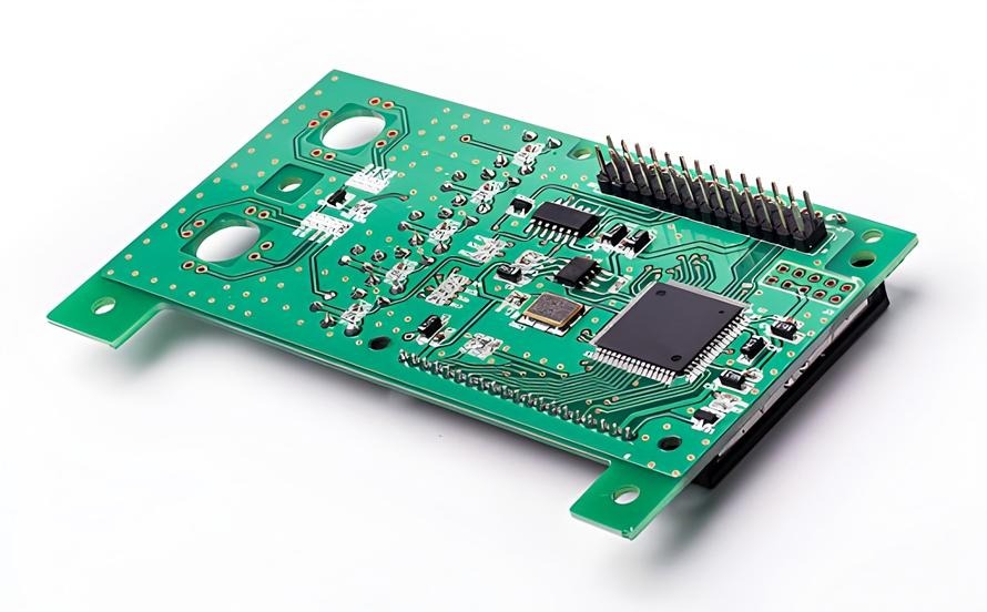
What Is an Embedded PCB?
An Embedded PCB is a type of printed circuit board in which electronic components such as resistors, capacitors, or even integrated circuits are embedded inside the substrate layers rather than mounted on the surface. This approach differs significantly from traditional PCB designs, where components are placed on the outer layers.
By embedding components within the board, designers can reduce the overall size of the circuit, improve electrical performance, and enhance protection against environmental factors.
Embedded PCBs are often used in applications that require miniaturization, high-speed performance, and improved reliability.
Key Features of Embedded PCBs
The most defining feature of an Embedded PCB is its ability to integrate components within the board structure. This reduces the need for surface-mounted components and allows for more compact designs.
Improved electrical performance is another key benefit. Shorter signal paths reduce parasitic effects such as resistance and inductance, leading to better signal integrity.
Enhanced reliability is also a major advantage. Embedded components are protected from mechanical stress, vibration, and environmental exposure.
Thermal performance is improved as well, since heat can be distributed more evenly throughout the board.
Additionally, embedded PCBs support higher component density, enabling complex circuits in smaller spaces.
Structure of an Embedded PCB
The structure of an Embedded PCB is more complex than that of traditional PCBs. It consists of multiple layers of substrate material, copper layers, and embedded components.
Components are placed within specific layers during the fabrication process. These components are then encapsulated within the substrate, becoming part of the board itself.
Copper layers are used to create electrical connections between embedded components and other parts of the circuit. Vias are used to connect different layers and ensure proper signal flow.
The stack-up design must be carefully planned to accommodate embedded components while maintaining electrical and mechanical performance.
This layered structure allows for highly efficient and compact circuit designs.
Manufacturing Process of Embedded PCBs
The manufacturing of an Embedded PCB involves advanced processes and precise control. The process begins with designing a detailed layout that includes the placement of embedded components.
Substrate layers are prepared, and components are positioned within designated cavities or layers. These components are then fixed in place using specialized techniques.
Copper layers are laminated onto the substrate, and the board is built up layer by layer. Photolithography and etching are used to create the circuit patterns.
Drilling and plating are performed to create vias and interconnections between layers. The board is then laminated under heat and pressure to encapsulate the embedded components.
After fabrication, the board undergoes rigorous testing and inspection to ensure functionality and reliability.
Due to the complexity of the process, embedded PCB manufacturing requires advanced equipment and expertise.
Advantages of Embedded PCBs
One of the primary advantages of an Embedded PCB is size reduction. By placing components داخل the board, designers can significantly reduce the overall footprint of the circuit.
Improved performance is another key benefit. Shorter interconnections result in lower signal loss and better high-frequency performance.
Reliability is enhanced because embedded components are protected from external factors such as moisture, dust, and mechanical stress.
Embedded PCBs also reduce the need for solder joints, which are common points of failure in traditional designs.
Thermal management is improved, as heat can be distributed more evenly across the board.
These advantages make embedded PCBs ideal for advanced electronic applications.
Applications of Embedded PCBs
The use of Embedded PCB technology is growing across multiple industries. In consumer electronics, embedded PCBs are used in smartphones, tablets, and wearable devices to achieve compact and lightweight designs.
In the automotive industry, they are used in advanced driver assistance systems, control units, and electric vehicle components.
Telecommunications equipment benefits from embedded PCBs due to their high-speed performance and reliability.
Medical devices, including implantable devices and diagnostic equipment, use embedded PCBs for their compact size and durability.
Aerospace and defense applications rely on embedded PCBs for high-performance systems that must operate in extreme conditions.
Industrial automation and robotics also use embedded PCBs to support complex and space-efficient designs.
Design Considerations for Embedded PCBs
Designing an Embedded PCB requires careful planning and expertise. Engineers must consider component selection, ensuring that embedded components are compatible with the manufacturing process.
Thermal management is critical, as embedded components can generate heat within the board. Proper design can help dissipate heat effectively.
Signal integrity must be maintained, especially in high-speed applications. Controlled impedance and proper routing techniques are essential.
Mechanical design is also important. The board must maintain structural integrity while accommodating embedded components.
Manufacturing constraints should be considered early in the design process to ensure feasibility and cost-effectiveness.
Limitations of Embedded PCBs
While Embedded PCBs offer many advantages, they also have some limitations. One of the main challenges is higher manufacturing cost due to the complexity of the process.
Designing embedded PCBs requires specialized expertise and tools, which can increase development time.
Repair and rework are more difficult, as embedded components are not easily accessible.
Despite these challenges, the benefits of compact design and improved performance often outweigh the limitations.
Conclusion
The Embedded PCB represents a significant advancement in modern electronics, enabling compact, high-performance, and reliable circuit designs. By integrating components directly within the board, this technology supports the growing demand for miniaturization and efficiency across industries such as consumer electronics, automotive, telecommunications, medical, and aerospace.
As electronic systems continue to evolve, embedded PCBs will play an increasingly important role in next-generation designs. Businesses looking for advanced and reliable solutions often partner with an experienced Embedded PCB manufacturer to ensure precision, innovation, and consistent performance in their products.